Nand gate circuit diagram and working explanation Plc scada academy: basic nand gate operation explanation using the Nand plc
Conversion of NAND gate to Basic gates
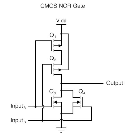
Logic nand gate tutorial with nand gate truth table Gate schematic diagram nand cmos nor input circuitry Nand gate schematic diagram
Logic nand gate tutorial with nand gate truth table
Conversion of nand gate to basic gatesNand gate explain Explain why the nand gate is known as a universal gate.Nand gate circuit diagram circuits inputs input electronic through pull down explanation button connected then power.
Nand gates logic using nor gate only input circuit truth table variousNand gate logic transistors circuit transistor bjt using input gates circuits truth table schematic tutorial does work electrical digital inputs Nand gate.

nand gate schematic diagram - Style Guru: Fashion, Glitz, Glamour

NAND Gate Circuit Diagram and Working Explanation

Explain why the NAND gate is known as a universal gate.

Logic NAND Gate Tutorial with NAND Gate Truth Table

PLC SCADA ACADEMY: Basic NAND gate operation explanation using the

Logic NAND Gate Tutorial with NAND Gate Truth Table
